
How To Design ESP32 Devboard with ESP32-WROOM-32
ESP32 has been very popular in the field of IoT. So today we will look at how to build an ESP32 Devboard.
Introduction
ESP32 has been very popular in the field of IoT. So today we will look at how to build an ESP32 Devboard. This is the minimum development board you can build with ESP32, so in the future, if you want to use ESP32 in your design, you can follow this guide to design the circuit and add other features you want.
We are using the official ESP32 DevKit as the reference because it already has the complete schematic PDF file and PCB layout PDF file. I know it is not as perfect as giving you the original design files. But it is good enough as you can already see many details.
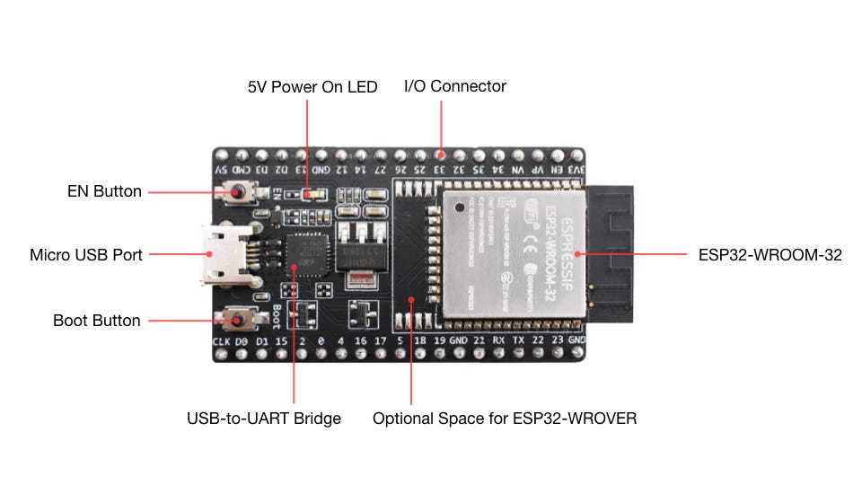
Let’s look at what this DevKit actually looks like.
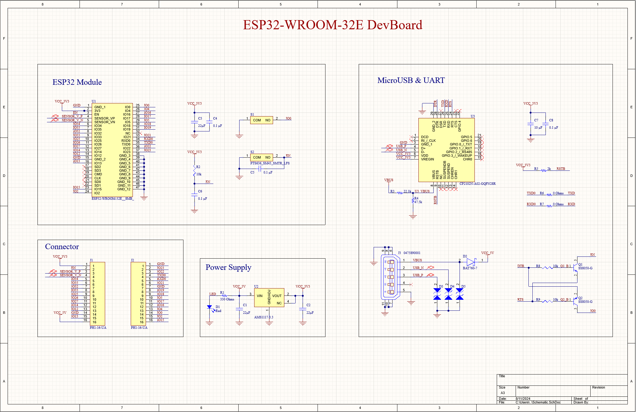
Schematic Overview
Here is the screenshot of the schematic:
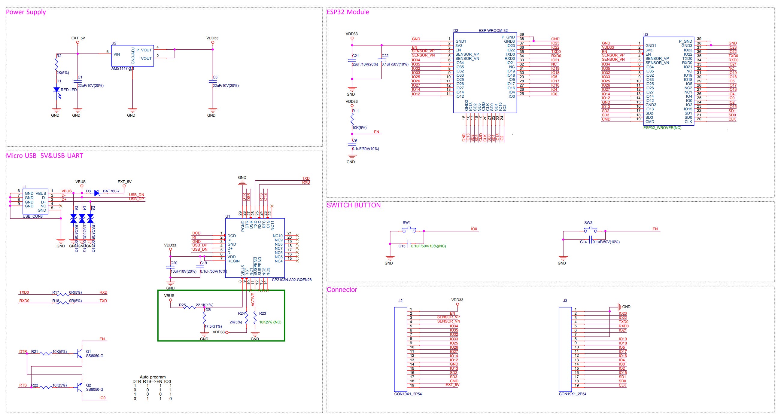
As we can see, it can be broken into five different parts.
Power Supply
ESP32 Module
Switch Button
Connector
Micro USB 5V & USB-UART
Power Supply
Let’s look at the power supply.
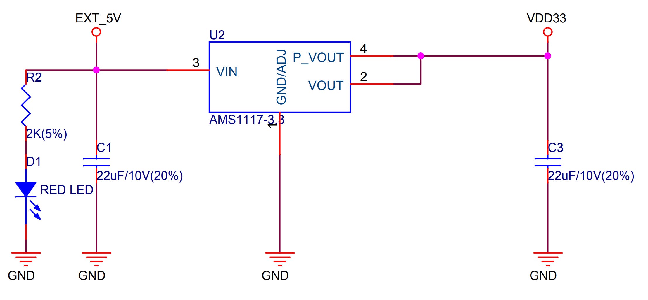
We can see that it uses an AMS1117-3.3 chip which is a very commonly used voltage regulator chip. The AMS1117-3.3 chip is part of the AMS1117 series chips with a fixed output voltage of 3.3V.
We can see from the datasheet that it can output up to 1A of current, and it has up to 0.2% of Line Regulation and 0.4% of Load Regulation.
The downside of this regulator is that since it is linear, it is not efficient. So, if you are designing a board that needs very strict thermal requirements, you should use a switching power supply.
But if you want to have an output voltage with a simple setup, this is the choice.
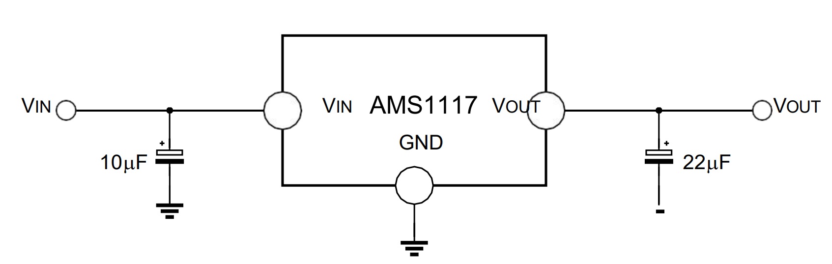
We can see from the datasheet below that only two filtering capacitors are required to complete the circuit.
The ESP32 DevKit uses an extra resistor and an LED to indicate whether the power is on or not. This is a smart trick for it shows the user clearly what is happening.
ESP32 Module
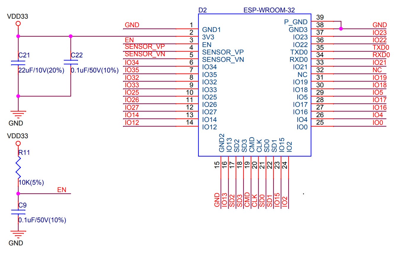
The board uses an older version of the ESP32 module, now it is updated to ESP32-WROOM-32E. Rest assured, these two chips are pin-compatible, so you can use the design here as well.
Switch Button
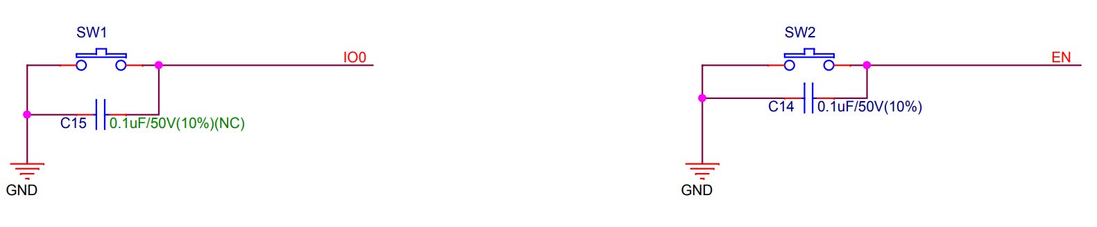
The switch button in this design is pretty easy. However, one thing to note here is that the C15 capacitor is not used in the design as it is causing problems. The C14 capacitor is here to act as a debouncer to filter out rapid fluctuation caused by the mechanical switch buttons.
Connector
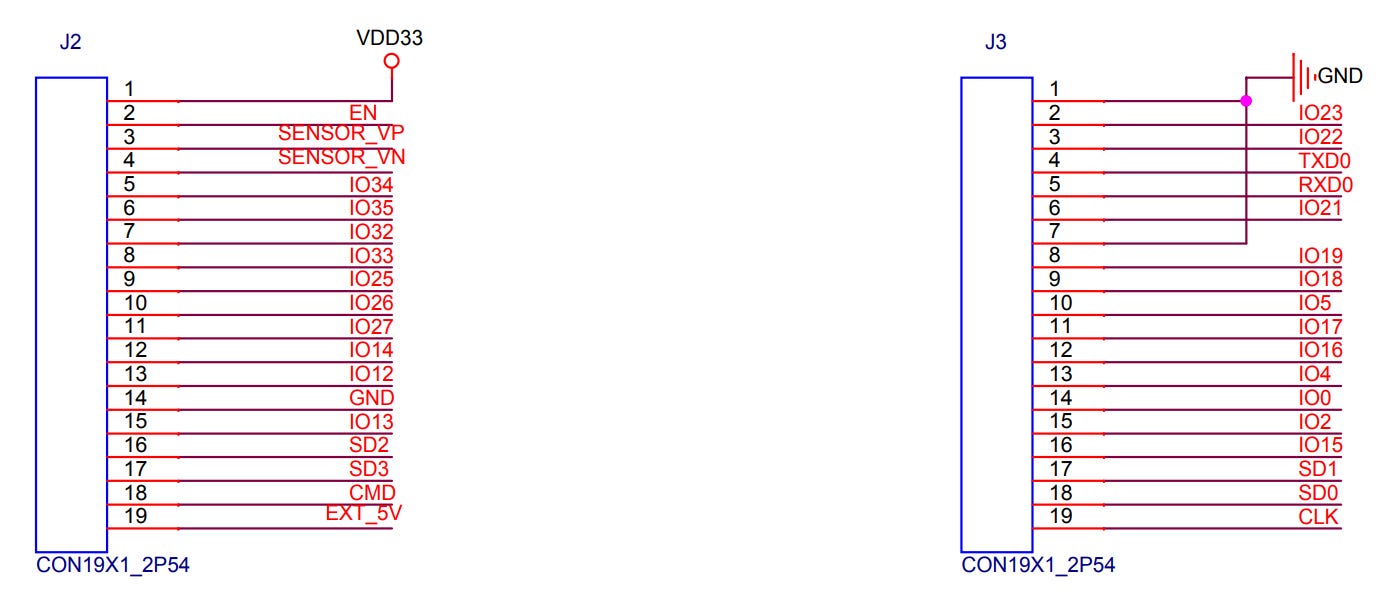
The DevKit has two connectors on both sides, each one has 19 pins. One thing to note here is that pins 16, 17, and 18 on the J2 and pins 17,18, and 19 on J3 are not recommended for connecting anything, because they are already connected to the internal embedded PSRAM according to the datasheets of both ESP32-WROOM-32 and ESP32-WROOM-32E.
So, if you are designing your own board, you can leave all these pins open or use connectors with fewer pins to reduce the board size.
Micro USB 5V & USB-UART
From the schematic, we can see that the DevKit uses Micro USB as its power and debugging port. However, the ESP32 doesn’t support USB, so it uses a chip to convert the USB to UART, which is CP2102N-A02-GQFN28.
The CP2102N-A02-GQFN28 is a very common chip used as the USB 2.0 to UART Interface.
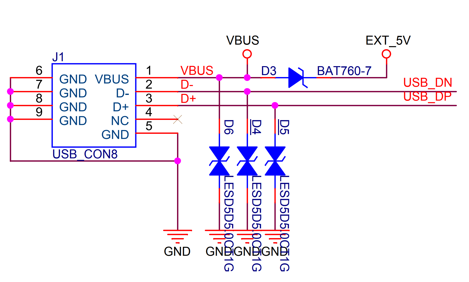
We can see from the Micro USB port that this port is responsible for supporting power for the entire board. And before it does that, there is a diode and a TVS diode for ESD protection. And there is a TVS diode for each of the USB differential inputs. This is a standard way of designing input circuits connected with external inputs.
The part number for the TVS diode is LESD5Z5.0CT1G. From the datasheet, I found that its total length is only 1.5mm, which is suitable for constrained board areas.
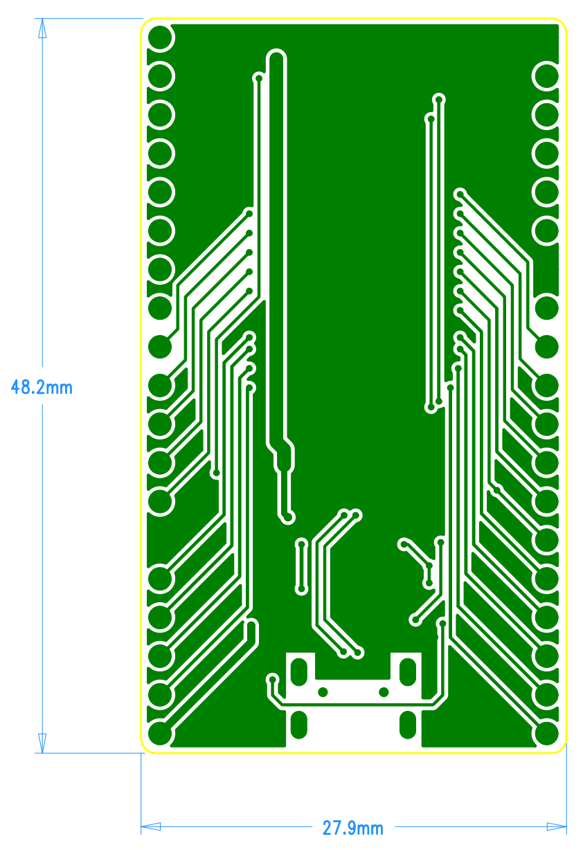
PCB Size
Let’s look at the size of the board.
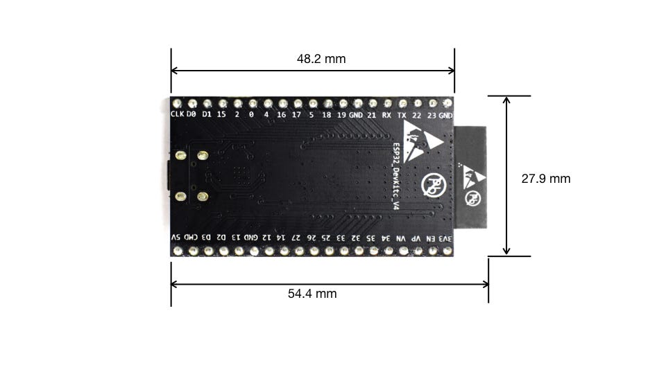
We can see that some parts of the ESP32 chip are sticking out of the board, which is to improve the WiFi and Bluetooth signal. The total length of the board is about 54.4 mm and the width is about 27.9 mm.
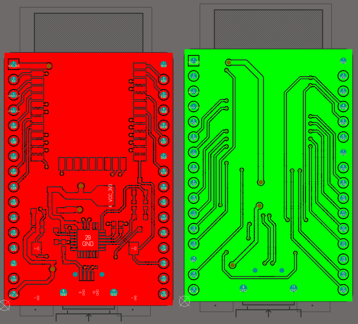
PCB Overview
Here are the screenshots of the PCB layout, and it only has two layers:
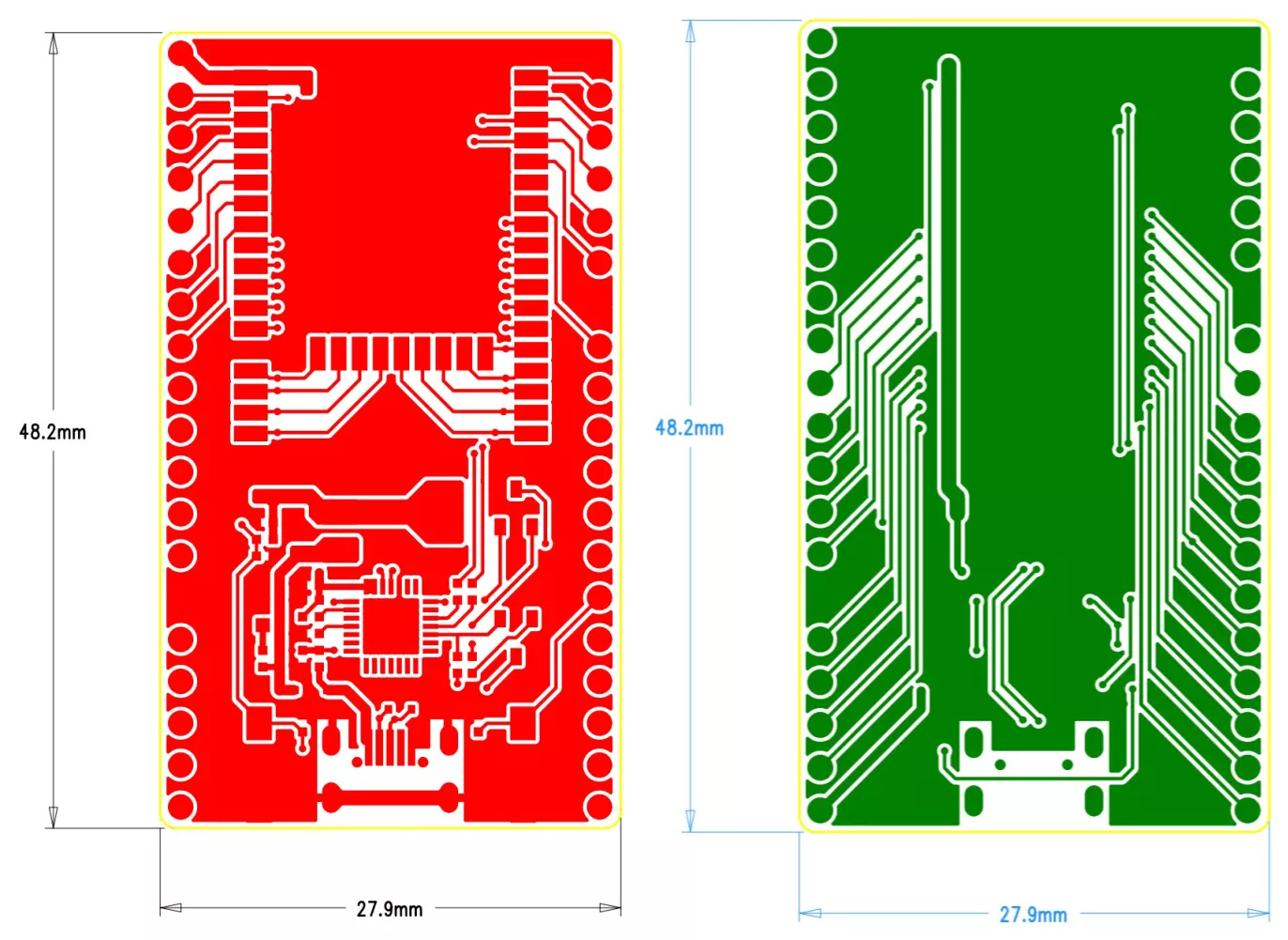
As we can see, both the top and bottom layers are filled with copper ground everywhere. This is common when you only have two layers and want to create a good return path for your signal and power.
The Top Layer
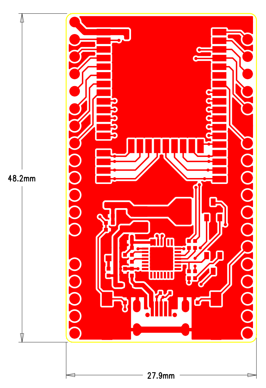
There are a couple of things we can see from the top layer.
First, both the 3.3V and 5V traces are much thicker than the signal traces, due to the reason that thicker traces can deliver more current which is not needed in the signal traces.
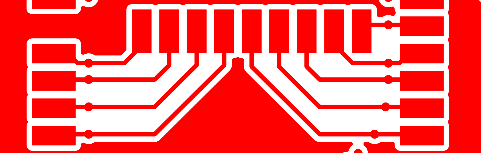
One thing I find very interesting is the part in the above picture. There are vias in the middle of the traces.
The Bottom Layer
As you can see, there is no component on the bottom layer, which makes the routing rather simple.
The 3.3V trace is also very thick.
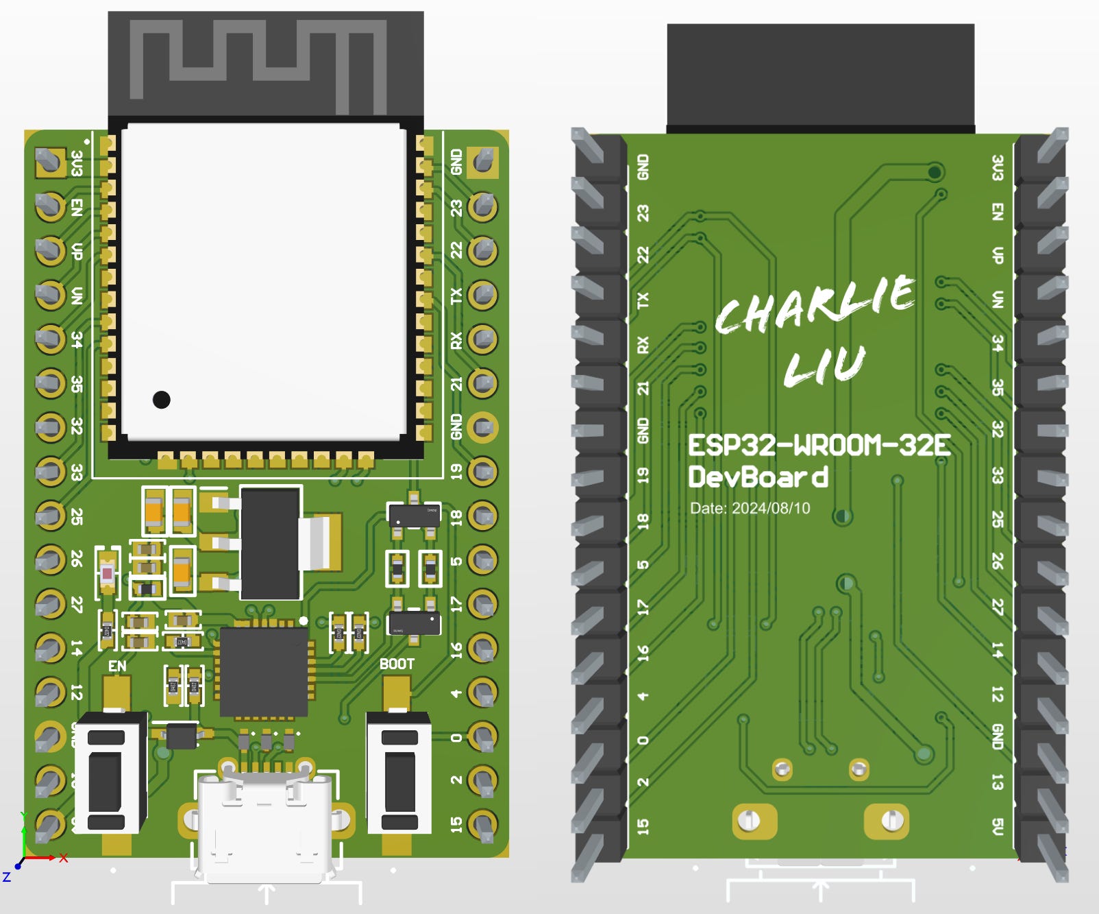
Making My Own Board
I am making my own board using the knowledge I learned from the reference design. The software I use is Altium Designer. In this design, I simplified both the schematic and the PCB, like using 16-pin headers instead of 19, which makes my board slightly smaller than the reference board. I also leave pins 16 to 21 open, as they don’t serve any use.
Here is the schematic.
Here is the PCB layout and 3D model.
I believe that after reading this article, you can also make your own ESP32 DevBoard and integrate ESP32 chips into your designs.
Reference
ESP32-DevKitC V4 Documentation
AMS1117 Datasheet - Advanced Monolithic Systems
ESP Modules | Espressif Systems